Mainstream MCU adaptation and feedback
Use this page to extend an exact STM32 or GD32 part without weakening the common
platform. The current iteration adds STM32F103RBT6 and GD32F303RCT6 reference
adaptations and extends selected G474, H743 and U575 modes. Implemented source
is separate from a passed software candidate. Every applicable physical result
remains not_executed until connected equipment executes its station plan.
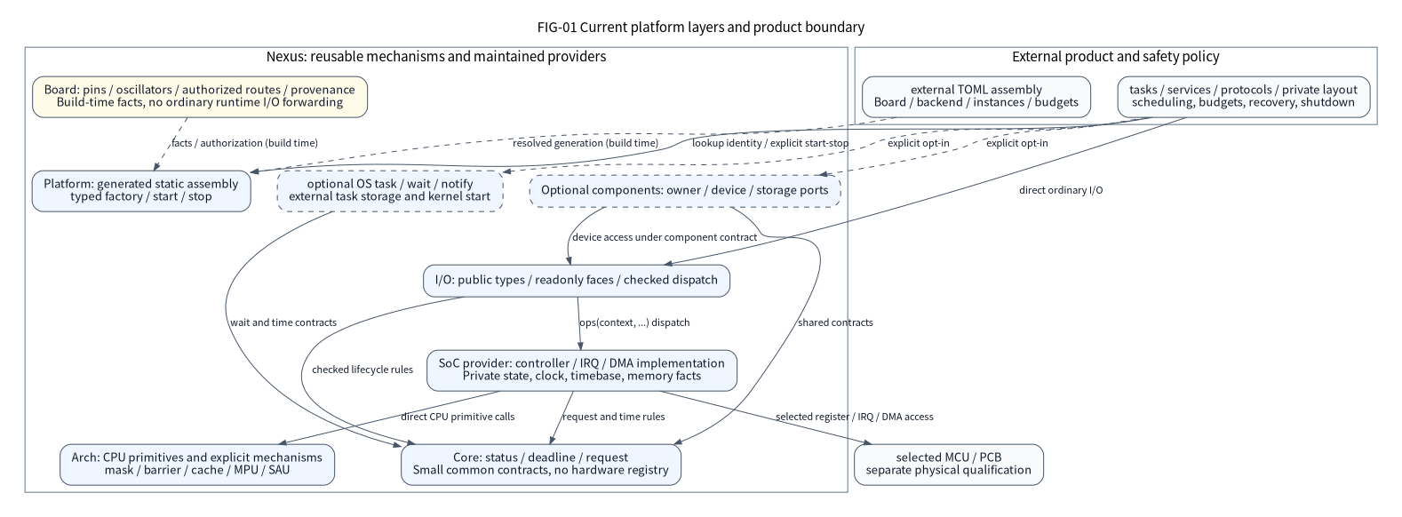
FIG-01 is the current responsibility diagram, not a claim that every peripheral or family is adapted. Its arrows express dependencies: products consume common interfaces; private SoC providers consume reviewed vendor operations. FIG-03 in the platform explanation describes TOML, facts, immutable IR, atomic generation and CMake selection. No additional runtime registry, default worker or mandatory OS layer is introduced here.
Finite parts and reference configurations
The exact-part table defines the adaptation boundary. Source implementations, reviewed chip routes, Board wiring, executed software qualification and physical measurements remain separate facts. Adding one entry does not enable every part with the same family prefix. Current facts, routes and capability derivation remain authoritative; this page is not another completion database.
Exact part |
Core and main memory |
Reference boundary |
|---|---|---|
STM32F407ZGT6 |
M4F; 1 MiB Flash; 128 KiB SRAM plus 64 KiB CCM |
Existing Qiming reference; only reviewed routes and selected modes |
STM32F407VET6 |
M4F; 512 KiB Flash; 128 KiB SRAM plus 64 KiB CCM |
Existing Sky reference; package and Board routes remain independent |
GD32F470ZGT6 |
M4F; 1 MiB Flash; 512 KiB across SRAM/TCM regions |
Existing Liangshan reference; separate GD32 SDK and provider |
STM32G474RET6 |
M4F; 512 KiB Flash; 96 KiB SRAM plus 32 KiB CCM |
Existing Nucleo reference; selected peripheral expansion in this iteration |
STM32H743ZIT6 |
M7; 2 MiB Flash; domain-specific RAM |
Fixed HSI/cache, finite USART3 DMA, optional initialized D2 SRAM1 and selected finite peripheral fixtures; separate V-revision HSI64 baremetal SPI4 DMA and continuous USART3 double-buffer RX with Cache off/on; Cache-off PLL384 references |
STM32U575ZIT6Q |
M33; 2 MiB Flash; domain-specific RAM |
TZEN0 finite peripherals, selected USART1 GPDMA TX, finite hardware-chain TX or bounded FIFO IRQ bytes; separate pinless LPTIM2 RUN one-shot and TZEN1 scalar GPIO/copied cooperative jobs |
STM32F103RBT6 |
M3; 128 KiB Flash; 20 KiB SRAM |
NUCLEO-F103RB source reference; HSI8, finite GPIO/UART/SPI/I2C/ADC/PWM/EXTI/Flash/IWDG selections |
GD32F303RCT6 |
M4F; 256 KiB code Flash; 48 KiB SRAM |
IRC8M chip reference with finite peripheral selections and TIMER1/TIMER4 time cascade; no invented PCB |
The H743 and U575 memory regions are not one interchangeable DMA heap. Consult
their exact soc.json memory domains and DMA contracts. Likewise, F407 CCM is
not ordinary DMA-accessible SRAM; GD32F470 TCM likewise has a separate reachability
contract. The GD32F303 RC part deliberately avoids the
larger-density code/data Flash split; another density requires its own geometry
and executable-memory review.
NUCLEO-F103RB wiring comes from UM1724 Rev 17: PA5 is D13/user LED LD2, and USART2 PA2/PA3 reaches ST-LINK VCP with SB13/SB14 ON and SB62/SB63 OFF. These are documented reference conditions, not observations of a connected board. The HSI profile does not assume the board’s optional HSE or ST-LINK MCO arrangement. GD32F303 pin multiplexing is a chip route until a separately sourced PCB authorizes the connection and electrical conditions.
Nine I/O classes and explicit rejection
This table describes the software scope to inspect, not executed qualification. “Selected” always means the controllers, routes and modes declared by the facts and fixtures. “Outside this increment” means configuration must reject that selection; a register header or upstream library is insufficient to accept it.
Public class |
F407 and F470 existing scope |
G474 increment |
H743 and U575 increment |
F103 and GD32F303 increment |
|---|---|---|---|---|
GPIO |
Selected inputs/outputs and safe initialization |
A/B/C/D/F/G package routes; PF0/PF1/PG10 reserved |
H743 selected GPIO; U575 A..G and H0/H1/H3 package routes, subject to power admission |
Selected legacy GPIO inputs/outputs; reviewed pin subsets only |
UART |
Selected IRQ, finite/continuous RX and DMA modes |
LPUART1, USART1/2/3 and UART4/5 IRQ bytes |
H743 USART3 IRQ, finite DMA TX/RX-IDLE and separate V/HSI64 baremetal continuous double-buffer RX; U575 USART1/2 IRQ bytes, selected finite USART1 GPDMA TX or hardware-chain TX; both families have separate bounded FIFO IRQ selections |
USART2/USART0 IRQ bytes, finite channel-DMA TX or duplex finite RX blocks |
SPI |
Selected byte and full-duplex DMA modes |
SPI1/2 finite polling; no DMA |
H743 SPI4 and U575 SPI1 finite polling; separate H743 V-revision HSI64 baremetal finite SPI4 DMA with Cache off/on |
F103 SPI1 and GD303 SPI0 finite polling |
I2C |
Selected polling and shared asynchronous engine |
I2C1 PB8/PB9 finite polling with HSI16 |
H743/U575 I2C1 PB8/PB9 finite V2 polling |
F103 I2C1/GD303 I2C0 PB6/PB7 IRQ messages, nominal 80 kHz, priority 0 without kernel notification |
ADC |
Selected one-shot, trigger and block modes |
ADC1 PA0/IN1 bulb shots or finite TIM6 normal-DMA blocks |
H743 ADC1 PA3/INP15 16-bit shots; U575 ADC4 PC0/channel1 12-bit shots with external supply admission |
PA0/channel0, 12-bit software shots at 4 MHz; explicit calibration and warmup |
PWM/timer |
Selected PWM, capture and advanced timer contracts |
TIM3/4 CH1 exclusive fixed-base PWM |
TIM3 CH1 PA6, exclusive fixed-base PWM |
F103 TIM3 CH1/GD303 TIMER2 CH0 PA6, exclusive fixed-base PWM |
EXTI |
Selected edges and shared IRQ ownership |
PA0/PA1 selected events |
PA0/PA1 selected events; U575 has separate rising/falling pending banks |
PA0/PA1 selected events on both exact parts |
Flash |
Selected geometry and caller-supplied region |
DBANK=1, unswapped; 512 KiB, 2 KiB pages, 8-byte ECC units |
H743 2 MiB/128 KiB sectors/32-byte units, Cache off; U575 TZEN0/SWAP0 2 MiB/8 KiB pages/16-byte units |
F103 128 KiB/1 KiB pages; GD303 256 KiB/2 KiB pages; both 2-byte halfwords |
Watchdog |
Selected irreversible watchdog lifecycle |
Independent IWDG |
U575 IWDG and H743 IWDG1 |
F103 IWDG and GD303 FWDGT |
CAN, USB, Ethernet, DAC and storage/protocol services are separate capabilities; the nine-class table does not include or qualify them. Unsupported controllers, routes, transfer modes and backends must fail during resolution. They must not fall back from DMA to polling or substitute a different controller or pin. The derived capability matrix and the existing SoC ledger retain their actual authority.
The optional Ethernet contracts also remain distinct. The original eth face
uses contiguous untagged frames and four-word descriptors. The separate
eth_frames selection uses eight-word descriptors,
scatter-gather frame loans, one in-band VLAN C-tag and MAC hardware-event
timestamps on exact F407/F470 RMII references. They cannot own the same MAC
simultaneously. Neither contract includes a protocol stack or network clock
synchronization, and software composition does not qualify PHY/PCB wiring.
H743 SPI4 DMA selects DEV_ID 0x450, REV_ID 0x2003 (V), fixed HSI64/default
trim, Cache off/on and baremetal. Its normal finite full-duplex requests borrow
non-overlapping TX/RX spans in selected initialized AXI SRAM. Cache off accepts
1..65535 bytes; Cache on requires exclusive complete 32-byte lines with aligned
addresses and lengths of 32..65504 bytes. DMA1 Stream2/3 remain separate from
optional USART3 Stream0 TX or Stream1 RX. PLL384, FreeRTOS, 16-bit, fixed
dummy/discard and multisegment SPI DMA are
outside that mode. See the H743 provider contract.
The separate H743 rx-dma-continuous mode uses USART3, DMA1 Stream1/request45,
DBM/CIRC and at least three equal caller-owned AXI SRAM buffers. It selects the
V revision, fixed HSI64, baremetal and Cache off/on. Task service replaces the
inactive bank before a conservative BRR/TIM2-derived deadline and performs Cache
maintenance outside the IRQ. A late or uncertain replacement, cache failure or
no FREE buffer stops production with visible loss; loans remain until actual
drain. IDLE closes this producer and publishes its drained prefix; a caller must
explicitly reinitialize the stream before restarting. TX remains finite IRQ,
not DMA duplex. Cache-on buffers own complete aligned 32-byte lines. The mode
accepts 32..65535-byte Cache-off buffers or 32..65504-byte Cache-on buffers.
It does not establish measured throughput, deadline or physical qualification.
U575 USART1 dma-tx selects TZEN0, MSIS4, 8N1, Cache off and finite nonsecure
SRAM1 payloads through GPDMA1 channel0/request25. IRQ-byte RX remains independent.
The GPDMA contract preserves ES0499 persistent DMAT,
separate UART wire TC and full source/IRQ/publisher drain. The independent
irq-fifo-bytes selection has explicit thresholds and per-IRQ
RX/TX byte budgets; it does not combine with DMA. These selections do not add
USART2 DMA/FIFO, RX DMA, LPDMA, TrustZone transport or autonomous
low-power execution.
The separate U575 dma-chain-tx mode uses the same USART1/GPDMA channel and
independent IRQ-byte RX. One request borrows a contiguous SRAM1 payload, up to
three blocks of at most 65535 bytes, and at most two packed 12-byte private
nodes. The 24-byte node array is 32-byte aligned within one CLBAR window. The
196605-byte protocol limit also requires actual reachable, nonaliasing RAM; it
does not reserve the whole SRAM for the caller. Payload and nodes remain live
until fetch/channel/IRQ drain and independently observed UART TC. This finite
selection does not enable scatter-gather or cyclic chains.
The independent pinless U575 LPTIM2 irq-counter16-oneshot reference selects
TZEN0, MSIS4, baremetal and PCLK1/4 for a nominal 1 MHz RUN counter. Requests
accept 2..65536 ticks; one tick is rejected because ARR must exceed reset CCR0.
IRQ68 priority5 never calls the OS. It owns no external pin or DMA and does not
promise Stop, backup or VBAT continuity. PCB and silicon revision remain
unobserved; software model and link checks do not measure physical timing.
Exact mode boundaries
G474 has 52 GPIO pads in the RE package, not six complete sixteen-pin banks. The fixed HSE profile reserves PF0/PF1; PG10 remains reserved because its NRST option is not changed. The GPIO inventory is independent of a Board connector route. SPI1/2 use eight-bit transfers, modes 0..3, explicit active-low CS and at most 256 bytes per finite call. The 170 MHz profile caps requested SCK at 42.5 MHz: divider two would exceed the datasheet limit. G474 also implements TIM3 CH1 PA6 AF2 and TIM4 CH1 PB6 AF2 as independent whole-controller PWM owners: fixed upcounting active-high base, integer clock divisor 1..65536, period 1..65535 and staged duty 0..period. Capture, complementary outputs, break, IRQ, DMA and shared timer channels remain outside this increment.
Those PWM limits describe counter arithmetic, not unconditional pad frequency. SPI/PWM use OSPEEDR=11. DS12288 Table56 at 30 pF limits pad toggling to 50 MHz at VDD 1.62..2.7 V and 120 MHz at 2.7..3.6 V; the logical 85 MHz waveform at period two is therefore conditional. The current profile does not establish GPIO supply, load or pulse suitability; Board qualification must do so.
Polling SPI returns only after wire drain and inactive CS are proved. If a post-admission reset or CS withdrawal cannot prove that state, the executor retains the caller buffers and controller/CS owners, masks interrupts and calls the platform fault observer. It parks if the observer returns; external product recovery must not return into released storage. Idle stop/recovery failures retain their separate retryable private leases.
H743 USART3 uses PD8/PD9 AF7 and normal, finite RX DMA blocks on DMA1 Stream1, DMAMUX1 channel 1 request 45. The owner services completion and rearms the next block; gaps are possible. This is not a circular or continuous receiver. Only the selected initialized AXI/SRAM1 domains are admitted. Cache-off blocks contain 1..65535 bytes. Cache-on blocks own complete, exclusive 32-byte cache lines, with aligned address and length and a maximum length of 65504 bytes. Source withdrawal, stable remaining count and post-invalidation precede publication. A borrowed consumer or failed detach retains the stream, cache and platform dependencies.
U575 adds USART2 PA2/PA3 AF7 and package-valid GPIO routes. PG[15:2] require an already established VDDIO2 supply and observed PWR clock/IO2SV configuration; the platform does not enable an unknown external rail. IO2SV is a configuration observation, not a measurement of rail voltage. TZEN0 remains the general platform profile. The separate TZEN1 reference also accepts cooperative GPIO jobs of at most eight PC7 commands copied into one Secure slot. SERVICE advances at most one command, POLL reads latched status, CANCEL preserves earlier effects and CONSUME releases only a terminal job. Tickets never wrap; no NS address survives a call. This provides neither a user-buffer loan nor general asynchronous or cross-security transport support.
F103 standalone admission checks the CPU-readable factory Flash density, not a debug-only device-group or revision value. ES096 Rev15 section2.2.2 reports zero from normal-software DBGMCU reads; group and revision therefore remain unobserved. The configured STM32F103RBT6 declaration and package still require separate integration evidence. See the F103 source boundary.
F103 uses USART2 PA2/PA3 and PA0/PA1 EXTI events. F103 SPI1 and GD303 SPI0 use default PA5/PA6/PA7 with explicit PA4 active-low CS, nominal 31.25 kHz..4 MHz, eight-bit words, modes 0..3 and at most 256 bytes per finite call. Their SPI assemblies cannot also select the PA5 GPIO/LED binding. F103 TIM2 is 16-bit at a nominal 1 MHz; its overflow service and mask interval must stay below 65.536 ms. GD303 cascades TIMER1 update TRGO into TIMER4 ITI0 and extends the high overflow, with a service interval below 2^32 nominal microseconds. This preserves low wraps across the stated 800 ms Flash erase bound; the timer-bridge carry propagation still needs physical observation. Neither profile establishes calibrated wall time or FreeRTOS tick catch-up after same-bank fetch stalls.
Mode resources, acquisition and physical Flash
F103 USART2 uses DMA1 channel7 for TX and channel6 for finite RX; GD303 USART0 uses DMA0 channel3/channel4. TX-only construction has the compact TX state and explicit IRQ-byte ring; duplex alone adds caller-supplied RX blocks. Both admit only declared SRAM spans of 1..65535 bytes. Memory TC does not settle TX before wire TC and source withdrawal. Finite RX publishes only after channel/DMAR withdrawal and stable count; owner service rearms a free block, so gaps and visible loss remain part of the contract. An unavailable replacement never authorizes overwriting a consumer loan. Their PB6/PB7 I2C uses priority-zero IRQ handling and rejects kernel notifications; bus voltage and pull-ups are external. The shared legacy engine remains the sole protocol owner.
G474 ADC1 selects single-ended 12-bit bulb sampling, SYSCLK/128 = 1.328125 MHz and sample code0. Software shots discard the first conversion and keep their explicit warmup and spacing guards. TIM6 finite normal-DMA blocks accept only 2.5–50 kHz rates that divide the 1 MHz trigger timebase exactly. Bulb aperture depends on the preceding EOC and next trigger, not SMPR alone. IRQ stops the trigger; service observes DMA/ADC withdrawal and ADEN clear before publication, then a later service rearms. The admitted SRAM1/2 domain excludes CCM aliases even though silicon can DMA through its 0x20018000 alias. The 32 KiB CCM counts once. See the exact G474 contract for errata and aperture bounds.
H743’s optional D2 SRAM1 has explicit budgeting, gate admission and startup DATA/BSS initialization; NOINIT stays caller-owned. DMA rechecks initialized AXI/SRAM1 and clock state before borrowing. H743 ADC1 provides 16-bit raw shots on PA3/INP15 with cut-specific boost and complete linearity calibration; U575 ADC4 provides 12-bit PC0/channel1 shots after external VDDA/ASV admission. F103/GD303 use 12-bit PA0/channel0 shots at 4 MHz, with part-specific warmup and calibration. These formats and declared reference voltages are not measured analog accuracy. Their exact selected PWM/EXTI routes and pin conflicts remain in support and the adjacent SoC contracts.
Physical Flash exposes the whole exact part, not a product partition. Authored
supply_mv is a mandatory software assumption where required, never a voltage
measurement. nx_flash_geometry_t.program_flags can set
NX_FLASH_PROGRAM_REQUIRES_FRESH_ERASE: each unit needs a successful erase and
no later programming pulse. All-FF readback cannot prove hidden ECC history;
failed/interrupted pulses consume the unit until its next successful erase.
Providers keep no implicit history bitmap. Zero flags do not waive a provider’s
own programming rules, and all-FF input units issue no pulse.
Every physical pulse first clears and observes stale error/completion state, then requires fresh completion after its actual busy/write-buffer drain. G474, U575 and F407 gate EOP latching with EOPIE; GD470 uses ENDIE for its end flag. Their polling owner exclusively leases a disabled/inactive FLASH IRQ while selected pulse interrupt bits are temporarily set; the NVIC never enables that vector. Cleanup removes pulse mode/enables, locks and observes pending withdrawal while preserving priority. Legacy F103/GD303 and H743 completion flags latch unconditionally under their register contracts; the interrupt-enable precondition is not inferred for them. H743 drains BSY/QW/WBNE and requires Cache off; U575 drains BSY/WDW in TZEN0/SWAP0.
Timeout prevents a later pulse but cannot abort one already started. Same-bank fetch/IRQ can stall, and a permanently busy controller never returns caller storage as completed. Product code owns writable erase-aligned regions, voltage, watchdog, execution placement and power-loss recovery. The common Flash adapter does not invent erase history. The maintained two-bank storage algorithm erases the inactive bank before a save, writes distinct full header/payload units and programs a separate commit unit last; a failed save requires reopen/recovery before a later save erases that target again.
Watchdog activation is irreversible, including a programming failure after the start command. Preparation failures retain any unwithdrawn LSI or debug lease for stop retry. Programmed nominal duration is distinct from physical minimum and maximum duration. GD303 and F470 datasheets provide nominal internal RC frequency without a reviewed min/max envelope: successful programming returns success with zero bounds; an enabled state query reports unsupported bounds while preserving enabled, irreversible and actual debug facts. U575 rejects prescaled LSI and requires a nominal minimum of 375 microseconds so RLR is at least two. Bounds from every other part retain their own datasheet conditions.
Official sources and version pairing
Manufacturer documents establish silicon facts. Libraries supply selected operations; examples help identify ordering but do not establish a universal platform contract. Retain the original notices and license inventory, lock exact bytes or Git commits, and include the selected source closure in the Source SDK. Official PDF URLs can change; a future download must match the recorded digest or undergo a new review.
Source |
Observed identity |
Primary use |
|---|---|---|
DS5319 Rev 20, July 2025 |
RB memory, LQFP64 pins, clock limits and 16-bit timers |
|
RM0008 Rev 21, February 2021 |
RCC, GPIO/AFIO, USART, DMA and TIM2 semantics |
|
ES096 Rev 15, March 2022 |
Revision applicability and affected peripheral behavior |
|
UM1724 Rev 17 |
F103RB identity, LED, VCP and solder-bridge conditions |
|
Rev 3.0, January 2024 |
RC code Flash, RAM, package and pin definitions |
|
Rev 3.4 |
RCU, legacy GPIO/AFIO, USART, DMA and timer semantics |
|
Rev 1.4, April 2026 |
Revision-specific ordering and operating limitations |
|
Firmware Library 3.0.3; manufacturer 7z archive |
Reviewed device definitions and peripheral operations |
The observed GD32F303 Rev 3.0 PDF is 2,394,885 B with SHA-256
08119c470f3e98df6a2448720d9307dc82dcc059244818ae76a95e4b5fe158b9.
The observed firmware 7z is 15,892,832 B with SHA-256
1cd66b58fc182ee6e2d2d98d78660bb0b822d642489997e9848d5ecb1f6657e1;
its extracted or nested archives have separate identities. The errata PDF is
259,206 B with SHA-256
5154b936ad2f7283fd5359dedfc137612666c0dc6af2734a5f325a609cbc459e.
A differently named archive or revision is not interchangeable with these bytes.
STM32CubeF1 v1.8.7
pins CMSIS Device F1 c8e9a4a4f16b6d2cb2a2083cbe5161025280fb22 and HAL
fee494a92b5ad331f92ad21f76c66a5cb83773ee. Independently tagged CMSIS v4.3.5
and HAL v1.1.10 are different commits and must not be described as this official
Cube pair. The imported dependency lock, selected files and actual compile/link
results determine the integration’s source identity and compatibility.
The existing F407 LL dependency remains governed by its lock and the official-driver integration contract. F1, G4, H7 and U5 do not inherit F4 driver qualification. GD32 libraries remain separate dependencies. Review each imported file’s license and hardware assumptions; register similarity does not establish either condition.
What Zephyr contributes
The reviewed comparison is
Zephyr v4.4.2,
commit dccb09599635bdff17633fa7e9dab014b91dce90. Its
west manifest
pins its own HAL dependencies. It is a design reference, not another Nexus
configuration authority or an assertion that Zephyr supports every selected part.
In particular, GD32F3x0 and GD32F30x are different peripheral families.
Reviewed upstream pattern |
Nexus application and limit |
|---|---|
Preserve generated static contexts and shared typed operations; factory remains cold lookup |
|
Model CTL0/CTL1 and MODER/AFR separately; preload output state before enabling its mode |
|
Validate shared remap conflicts during generation; do not treat legacy remap as independent per-pin AF |
|
Use resolved bus/kernel clock facts for baud calculation; do not assume CPU frequency |
|
Keep DMA completion, wire completion and final settlement distinct |
|
Reject an unsupported memory domain or implement explicit whole-cache-line ownership and maintenance |
|
Reject unsupported chaining, widths and address adjustments before retaining references |
Nexus does not copy mandatory kernel integration, workqueues, device PM or runtime discovery into the default MCU path. An upstream driver may have a different timeout, cancellation or buffer-return contract. Retain Nexus absolute deadlines and the accepted-borrow contract; reusing register operations must not introduce a second transfer owner. Preserve upstream notices when copying code; an architectural comparison does not itself import source.
Acceptance sequence and next admissions
Each adaptation follows the same sequence: source/license review; failing configuration and real-provider tests; minimal implementation; passing tests; strict resource/mode rejection; ARM image/resource checks; relocated SDK consumption; and clean-source candidate qualification. Preserve the actual RED failure and GREEN commands. GoogleTest/GoogleMock remain host-only; firmware remains C11 and allocation-free by default. The qualification contract defines the evidence requirements rather than the number of files or checks in this page.
Exercise partial start failure, retry, reverse cleanup, instance isolation,
accepted cancellation, late IRQ and failed drain wherever the selected mode can
reach them. A failed drain retains QUARANTINED storage; a timeout never revokes
the borrow. Only acquire-observed SETTLED, after required references detach,
ends the provider’s access. The caller still drains its observers and controls.
The physical station separately observes chip/revision, Board/bridges, clock, image, reset and I/O behavior. Performance statements require the same image, clock, workload and instrument. Host test time and operation counts are not MCU cycles, IRQ latency, electrical correctness or safety qualification. Record hardware-dependent exits as pending while no equipment is connected.
Further mainstream candidates include STM32F072RBT6, STM32F303RET6, STM32G071RBT6, STM32L476RGT6 and GD32E230F8P6. These are proposed admission targets, not supported parts. Confirm official package/memory facts, source licenses, toolchain/ABI, a finite peripheral set and a separately sourced Board before implementation. Other GD32F4xx and STM32F4 parts likewise need explicit variant facts and routes; neither an SDK header nor matching core grants support.
Bootloader handoff, runtime reclocking, deep STOP, generic cross-domain DMA and broader U575 asynchronous transport retain their separate exits in the SoC refinement ledger. This iteration does not close those tasks by adding an MCU family or linking an official library.